products details

Created with Pixso. Home Created with Pixso. Products Created with Pixso.
Semiconductor PCB
Created with Pixso.

Turnkey Assembly Semiconductor PCB Printed Circuit Board Green Solder Mask

Turnkey Assembly Semiconductor PCB Printed Circuit Board Green Solder Mask

Brand Name: Ben Qiang
Model Number: FR-4/Rogers
MOQ: 1PCS
Price: custom made
Payment Terms: Bank Transfer/Alipay/PayPal
Supply Ability: 200,000 square meters/year
Detail Information
Place of Origin:
Shenzhen, China
Certification:
ISO/TS16949/RoHS/TS16949
Usage:
OEM Electronics
Special:
Blind Microvias
Layer Count:
36
Surface Finish:
Gold Plating 30U"
Material:
FR-4
Min Hole Size:
0.2mm
Pcba Service:
Turnkey Assembly PCB Service
Solder Mask Color:
Green
Packaging Details:
Air bead vacuum packaging
Supply Ability:
200,000 square meters/year
Highlight:

Turnkey Assembly Semiconductor PCB

,

Semiconductor PCB Green Solder Mask

,

Printed Circuit Board Green Solder Mask

Product Description

Turnkey Assembly PCB Service Printed Circuit Board For Semiconductor Green Solder Mask Color

Product Description:

Product Overview: Semiconductor PCB

The Semiconductor PCB, also known as Printed Circuit Board for Semiconductor or PCB For Semiconductor, is a specialized type of circuit board designed specifically for electronic devices that use semiconductors. It is a crucial component in the manufacturing process of these devices, as it provides a stable and reliable platform for the semiconductor components to be mounted onto.

Special Feature: Blind Microvias

One of the key features of the Semiconductor PCB is the inclusion of Blind Microvias. These are small, laser-drilled holes that connect different layers of the board, allowing for a more compact and efficient design. This feature is especially important in semiconductor devices where space is limited, as it allows for a higher density of components to be placed on the board.

Layer Count: 36

The Semiconductor PCB has a layer count of 36, which refers to the number of copper layers on the board. This makes it ideal for simpler electronic devices that do not require a high number of layers for their circuitry.

Testing Service: Function Test, 100% Test

To ensure the highest quality and functionality of the Semiconductor PCB, we offer both function testing and 100% testing services. This means that each board is thoroughly tested for its intended function, as well as for any potential defects or faults, before being delivered to the customer.

Usage: OEM Electronics

The Semiconductor PCB is primarily used in Original Equipment Manufacturer (OEM) electronics, where it serves as the main platform for the semiconductor components. It is commonly found in a variety of electronic devices such as smartphones, computers, and other consumer electronics.

Min Trace Width: 0.1mm

The minimum trace width of the Semiconductor PCB is 0.1mm, which refers to the width of the copper traces that connect different components on the board. This allows for a more precise and compact design, making it suitable for smaller and more intricate electronic devices.


Features:

  • Product Name: Semiconductor PCB
  • Solder Mask Color: Green
  • Surface Finish: Gold plating
  • Usage: OEM Electronics
  • Drilling Size: Min 0.0078”(0.2mm)
  • Min Hole Size: 0.2mm
  • Circuit Board for Semiconductor
  • Board for Semiconductor
  • Circuit Board for Semiconductor Manufacturing
 

Technical Parameters:

Printed Circuit Board for Semiconductor  
Solder Mask Color Green
Min Hole Size 0.2mm
Material FR-4
Through Hole Technology No
Lead Time 2 Weeks
Surface Finish Gold plating
Pcba Service Turnkey Assembly PCB Service
Feature High TG
Testing Service Function Test, 100% Test
Impedance Control No
Printed Circuit Board for Semiconductor  
 

Applications:

Semiconductor PCB - Perfect Solution for Semiconductor Industry

Introduction

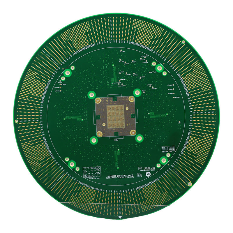
Semiconductor PCB, also known as PCB for Semiconductor, is a type of printed circuit board specially designed for the semiconductor industry. It is used in various applications related to the production, testing, and operation of semiconductor equipment.

The PCB for Semiconductor industry is made with high precision and quality to meet the demanding needs of the semiconductor manufacturing process. It is a crucial component in the production of semiconductors and plays a vital role in ensuring the efficiency and reliability of semiconductor equipment.

Product Features
  • Drilling Size: Min 0.0078”(0.2mm) - The drilling size of the Semiconductor PCB is highly precise, allowing for the creation of small holes and microvias for the placement of electronic components.
  • Special: Blind Microvias - This feature enables the creation of microvias that are only visible on one side of the PCB, making it ideal for complex and compact semiconductor equipment designs.
  • Testing Service: Function Test, 100% Test - The PCB for Semiconductor undergoes rigorous testing to ensure its functionality and reliability in the semiconductor production process.
  • Layer Count: 36  - With 36 layers, this PCB provides a compact and efficient solution for the complex wiring and electronic components placement required in semiconductor equipment.
  • Material: FR-4 - This high-quality flame-retardant material is widely used in the semiconductor industry due to its excellent electrical and mechanical properties.
Application and Scenarios

The Semiconductor PCB is widely used in various applications and scenarios in the semiconductor industry. Some of the most common ones include:

  • Semiconductor Production - The PCB for Semiconductor is an essential component in the production of semiconductors. It is used in various stages of the manufacturing process, from etching and plating to testing and packaging.
  • Semiconductor Testing - As the PCB is a critical part of semiconductor equipment, it also undergoes testing to ensure its functionality and reliability. The Semiconductor PCB plays a crucial role in this process, providing accurate and stable results.
  • Semiconductor Equipment Operation - The PCB for Semiconductor is an integral part of the operation of semiconductor equipment. It provides the necessary electrical connections and supports the functioning of electronic components in the equipment.
  • Semiconductor Equipment Maintenance - The PCB for Semiconductor is also used in regular maintenance and repairs of semiconductor equipment. Its high precision and quality ensure the smooth and efficient operation of the equipment.
Conclusion

The Semiconductor PCB is an essential product for the semiconductor industry, providing a reliable and efficient solution for the production, testing, and operation of semiconductor equipment. With its high precision, quality, and special features such as blind microvias, it is the perfect solution for any semiconductor application or scenario. Choose Semiconductor PCB for your semiconductor equipment and experience unparalleled performance and reliability.


Customization:

Semiconductor PCB Customization Service

Product: Semiconductor Circuit Board

Impedance Control: No

Layer Count: 36

Drilling Size: Min 0.0078”(0.2mm)

Through Hole Technology: No

Min Hole Size: 0.2mm

Customize Your Circuit Board for Semiconductor

At Semiconductor PCB, we understand the unique needs of semiconductor devices and offer customized solutions for your circuit board needs. Our customizable services include:

  • Layer Count: Our boards are designed with 36 layers to meet the specific requirements of semiconductor devices.
  • Drilling Size: With a minimum drilling size of 0.0078”(0.2mm), our boards provide precise and accurate placement of components.
  • Through Hole Technology: Our boards do not utilize through hole technology, ensuring a compact and efficient design for your semiconductor device.
  • Min Hole Size: We offer a minimum hole size of 0.2mm, providing the necessary space for smaller components in your semiconductor device.

Choose Semiconductor PCB for a customized circuit board that meets the unique needs of your semiconductor device. Contact us today to learn more about our customization services.


Packing and Shipping:

Semiconductor PCB Packaging and Shipping

Thank you for choosing our Semiconductor PCB product. To ensure the safe delivery of your order, we have carefully designed our packaging and shipping process.

Packaging

Our Semiconductor PCBs are individually wrapped in anti-static bags to prevent any damage from static electricity. They are then placed in a sturdy cardboard box with foam padding to provide extra protection during shipping.

In addition, we use bubble wrap to secure the box and prevent any movement during transit. This helps to prevent any potential damage to the PCBs.

Shipping

We offer worldwide shipping for our Semiconductor PCBs. Our preferred shipping method is through reputable courier services such as DHL, FedEx, or UPS. This allows for fast and reliable delivery of your order.

For international orders, we carefully fill out all necessary customs forms and declarations to ensure smooth customs clearance. This may include providing information on the value and contents of the package.

Once your order is shipped, you will receive a tracking number via email so you can easily track the status of your delivery.

Please note that any additional taxes or duties imposed by the destination country are the responsibility of the customer.

Conclusion

With our secure packaging and reliable shipping methods, you can trust that your Semiconductor PCBs will arrive safely and in perfect condition. If you have any further questions or concerns, please do not hesitate to contact us.